

Abstract
A strain characterization method with nanoscale spatial resolution called cathodoluminescence is explained. The method involves the use of a small electron probe with high energy. The energy loss by the primary electrons results in the emission of light which are collected by reflective optics and detected by a spectrometer. By measuring the cathodoluminescence spectrum during scanning, a spatial map of the stress distribution can be deduced. This is because stress affects the peak of the emission spectrum from the sample via the piezospectroscopic effect. By monitoring the peak shift, the strain can be deduced from the piezospectroscopic coefficients. This method is especially useful for ceramic materials such as oxides and glasses for which the Raman effect is extremely weak. However, stress distribution in epitaxial III-nitride semiconductors had also been studied.
Keywords: Cathodoluminescence, Scanning electron microscope, Piezospectroscopic effect, III-nitride, optical glasses.
Related Journals
Recent Patents on Space Technology
Recent Progress in Space Technology (Discontinued)
Recent Patents on Engineering
Recent Patents on Mechanical Engineering

Current Alternative Energy

Recent Patents on Electrical Engineering

Recent Patents on Electrical & Electronic Engineering

Recent Advances in Electrical & Electronic Engineering
Related Books

6G Wireless Communications and Mobile Networking

Recent Advances in Renewable Energy

Recent Advances in Renewable Energy

Recent Advances in Renewable Energy
Recent Advances in Renewable Energy

Recent Advances in Renewable Energy

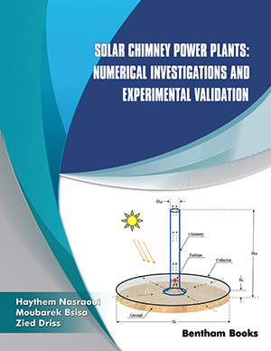
Solar Thermal Systems: Thermal Analysis and its Application

Recent Developments in Artificial Intelligence and Communication Technologies

40 YEARS OF SHS: A LUCKY STAR OF A SCIENTIFIC DISCOVERY A Presentation with Elements of a Scientific Lecture
A Review: Chill-Block Melt Spin Technique, Theories & Applications